
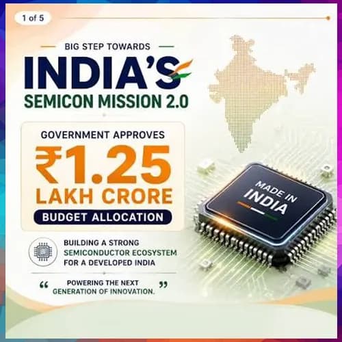
Industry body says official notification of the ₹1,27,500 crore scheme marks a shift from policy credibility to industrial capability, citing 12 approved projects, 60,000 students trained and rising VC funding as early proof points of India's semiconductor ambitions.
The India Electronics and Semiconductor Association (IESA) has welcomed the official notification of Semicon 2.0, calling it a significant step in strengthening India's semiconductor design and manufacturing ecosystem. The scheme, which carries a total budget outlay of ₹1,27,500 crore, builds on the earlier Semicon India Programme and is structured around six core pillars: chip design, machines and materials, new fabs, ATMP/OSAT, R&D and talent development.
IESA said the approach could deepen India's semiconductor capabilities, draw large-scale investment, generate high-value employment and reinforce the country's position as a trusted global semiconductor partner.
Policy continuity provides confidence for long-term investment
Ashok Chandak, President of IESA and SEMI India, said, “The official notification of Semicon 2.0 is a very significant milestone. The speed with which the Government has moved from Cabinet approval to official notification sends a strong message of policy continuity, execution and commitment. For an industry that makes investments with a 10–15 year horizon, this continuity provides the confidence required for long-term investments. India is now moving from credibility to capability—and policy continuity will be a key enabler of this journey .The first phase of this program already created confidence by 12 approved projects, 100+ Design start Up’s support, 355+ institutes/60000 students having EDA tools availability.
“What makes Semicon2.0 particularly significant is its end-to-end approach. The six pillars cover the semiconductor value chain—from chip design and fabs to ATMP/OSAT, machines and materials, R&D and talent. This is not simply about building semiconductor factories; it is about building the ecosystem around them and creating sustainable capabilities in India. In today’s notification further detailing of the Semicon2.0 focus areas, financial incentives and scheme were narrated for all six pillars and each of them is already showing traction. From chips for strategic sectors identified under the PSA and NSA's expert committee, to 70,000 students already trained under Chips to Startup and ₹1,000+ crore in VC funding already flowing to Indian design companies – these are credible proof points for the ecosystem that self-reliance is built brick by brick and Semicon 2.0 is a nation building exercise.”
Scheme could catalyse over ₹5 lakh crore in investment
Chandak said, “Based on the current investment pipeline and the much broader scope of Semicon 2.0, IESA sees the potential for the programme to catalyse more than 5 lakh crore of cumulative private and industry investment over the next five to seven years, across fabs, ATMP/OSAT, equipment and materials, design, R&D and the wider supply chain. R&D Focus on 7-3 nm pathway, Silicon photonics, Micro LED’s , Compound semiconductors and support to OCI and large corporates in fabless sector and manufacturing related skilling is notable differentiations .”
IESA noted that government financial support should be viewed as a catalyst rather than the total investment, since each semiconductor project generates a multiplier effect across equipment, materials, chemicals, precision engineering, packaging, testing, logistics and talent — an effect that grows further when combined with the ECMS, MPMS and EMC schemes.
The body described its long-term aspiration as building a "virtuous semiconductor and electronics flywheel," in which design drives IP and products, fabs and packaging build manufacturing capability, equipment and materials strengthen the supply chain, and electronics manufacturing creates demand that fuels further investment and innovation.
Convergence with broader electronics manufacturing push
IESA also pointed to the importance of aligning Semicon 2.0 with India's wider electronics manufacturing initiatives, including the Electronics Components Manufacturing Scheme (ECMS), Mobile Phone Manufacturing Scheme (MPMS) and Electronics Manufacturing Clusters (EMC).
“Semicon 2.0, together with ECMS, MPMS and EMC, creates an integrated policy architecture where semiconductors and electronics can feed and strengthen each other. This can accelerate domestic value addition, create opportunities for startups and MSMEs, attract global suppliers and enable India to move progressively from manufacturing for the world to creating and owning technology for the world,” Chandak added.
IESA credits MeitY and ISM leadership
The association congratulated Union Minister Ashwini Vaishnaw, MeitY Secretary S. Krishnan, and India Semiconductor Mission CEO Amitesh Kumar Sinha, along with the wider MeitY–ISM team, for their leadership and speed of execution.
“IESA appreciates the leadership of MeitY and ISM in moving swiftly from policy approval to notification. This combination of vision, continuity and execution is creating confidence across the semiconductor ecosystem. It gives domestic and global investors greater visibility to plan long-term investments in India.”
IESA reaffirmed its commitment to working with MeitY, ISM, state governments, industry and academia through initiatives such as Startup Mitra, Workforce Development, industry-led R&D via IDSPS, policy advocacy and international collaborations.
“The real success of Semicon 2.0 will not be measured by the number of fabs alone. It will be measured by the IP and products we create, the companies we build, the talent we develop, the value we retain and the global markets we serve. The aspiration should be to take India from policy credibility to industrial capability, from capability to scale, and ultimately to global technology leadership”, Mr. Chandak said.
The six pillars: Industry's 2030–32 ambitions
IESA outlined the following aspirations under each pillar, describing them as industry outlooks meant to complement the government's Semicon 2.0 objectives:
· Chip Design: Hundreds of fabless semiconductor companies by 2030–32, with 5–10 globally scaled product companies and 500+ indigenous IP/products.
· New Fabs: Seven or more additional operating/specialty fabs across silicon (logic and memory), compound and other strategic technologies, including entry into the 7nm node.
· ATMP/OSAT: Doubling of globally competitive advanced-packaging and testing capabilities.
· Machines & Materials: A large pool of Indian equipment, materials and precision-engineering companies, with 10–15 companies aspiring to become global suppliers.
· R&D: Major R&D centres/centres of excellence generating 100+ commercially relevant indigenous technologies and IPs.
· Talent Development: A workforce of several lakh people skilled across chip design, manufacturing, equipment, materials, advanced packaging and R&D by 2030–32.
IESA said these targets represent industry aspirations rather than government commitments, intended to give the ecosystem a measurable direction alongside the official Semicon 2.0 objectives.