
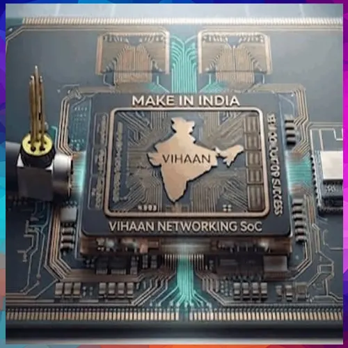
Chennai-based Aheesa Digital Innovations has successfully validated its VIHAAN networking SoC, developed using the indigenous VEGA microprocessor, with the company now preparing to move the fibre broadband chip towards production in 2027.
India’s domestic semiconductor design ecosystem has recorded another milestone with Chennai-based fabless startup Aheesa Digital Innovations achieving first-pass silicon success for its broadband networking System-on-Chip (SoC), VIHAAN.
Supported under the government’s Design Linked Incentive (DLI) Scheme, VIHAAN has been developed for fibre broadband applications and incorporates the indigenous VEGA microprocessor. The Ministry of Electronics and Information Technology (MeitY) said the successful silicon outcome marks an important stage in the chip’s development and paves the way for its transition towards production.
Aheesa taped out the VIHAAN design on Republic Day and achieved first-pass silicon success on Independence Day this year. The company is now preparing for the next stage, with production tape-out planned for 2027.
DLI scheme strengthens domestic chip design
The achievement comes as government-backed programmes seek to expand India’s capabilities across the semiconductor value chain. According to MeitY, startups supported through the DLI Scheme have collectively completed more than 30 chip design tape-outs across multiple foundries and attracted more than $100 million in venture capital investment.
Aheesa has also raised around Rs 40 crore this year from the Tamil Nadu Infrastructure Fund Management Corporation through the Tamil Nadu Emerging Sector Seed Fund, along with other private investors. The capital is expected to support product development and the company’s expansion in semiconductor design.
The government has highlighted chip design as a major source of value creation in the semiconductor industry. It estimates that design can account for up to half of the overall value addition across the semiconductor value chain and represents roughly 15-35% of the bill of materials cost of electronic products.
The DLI programme is supporting Indian startups developing semiconductor solutions for a broad range of applications, including satellite communications, drones, defence systems, automobiles, IoT, AI, telecommunications and smart metering.
Expanding design and innovation pipeline
Government semiconductor initiatives are also widening access to chip-design infrastructure. MeitY said electronic design automation tools have been provided to 455 organisations, comprising 350 academic institutions and 105 startups.
Under the Chips to Startup (C2S) Programme, 71 academic institutions have collectively taped out 245 chip designs. The initiative is intended to strengthen India's semiconductor talent pipeline and prepare skilled professionals for the industry’s future requirements.
Other recent achievements cited by the ministry include first-pass silicon success for a brushless DC motor controller developed by Vervesemi Microelectronics and successful testing of a 12nm Vision SoC from Netrasemi.
The government is seeking to build an integrated semiconductor ecosystem spanning chip design, fabrication, advanced packaging, equipment, materials, R&D and skilled manpower. The effort is set to receive further momentum from Semicon 2.0, approved in July 2026 with an outlay of Rs 1,27,500 crore, as India seeks to establish a globally competitive semiconductor industry.

See What’s Next in Tech With the Fast Forward Newsletter








Tweets From @varindiamag
Nothing to see here - yet
When they Tweet, their Tweets will show up here.